IBM Research
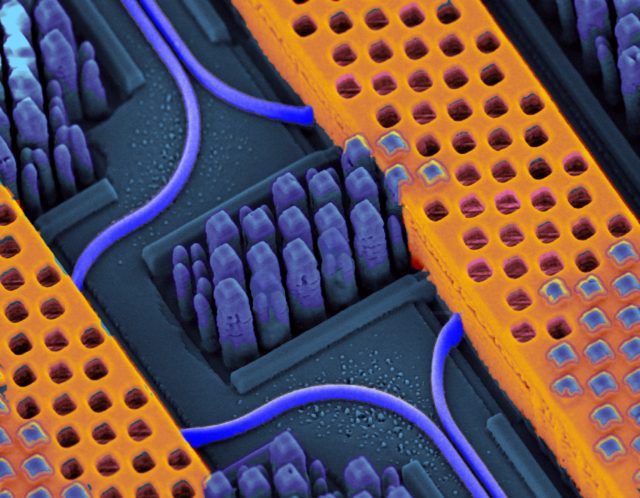
IBM has developed a technology that integrates optical communications and electronics in silicon, allowing optical interconnects to be integrated directly with integrated circuits in a chip. That technology, called silicon nanophotonics, is now moving out of the labs and is ready to become a product. It could potentially revolutionize how processors, memory, and storage in supercomputers and data centers interconnect.
Silicon nanophotonics were first demonstrated by IBM in 2010 as part of IBM Research's efforts to build Blue Waters, the NCSA supercomputer project that the company withdrew from in 2011. But IBM Research continued to develop the technology, and today announced that it was ready for mass production. For the first time, the technology "has been verified and manufactured in a 90-nanometer CMOS commercial foundry," Dr. Solomon Assefa, Nanophotonics Scientist for IBM Research, told Ars.
A single CMOS-based nanophotonic transceiver is capable of converting data between electric and optical with virtually no latency, handling a data connection of more than 25 gigabits per second. Depending on the application, hundreds of transceivers could be integrated into a single CMOS chip, pushing terabits of data over fiber-optic connections between processors, memory, and storage systems optically over distances ranging from two centimeters to two kilometers.
Cheap and scalable, the technology could have a huge impact on how data
centers for public cloud computing and other "exascale" applications—and the
computers in them—are built. Eventually, it could find its way into processors
themselves, though the low cost of 90-nanometer chips makes them "the most
cost-effective solution looking into the next decade," Assefa said.
For many distributed applications—such as Hadoop-based data analysis, video, and image processing—the greatest limiting factor is often the network, as information flows between processors. Network connections are also expensive, as they rely on additional hardware to manage them.
But direct optical connections could change the architecture of the systems built for these applications. They could be integrated into data center racks, allowing the components of servers to be set up in different physical units without a loss of performance. It could also allow for much more efficient and redundant storage networking. "Once you have this sort of universal technology," Assefa said, "it provides a lot of different kinds of bandwidth capability. "
For now, IBM is not making any announcements about actual product based on CMOS silicon nanophotonics. Assefa would not say if IBM intends to license the technology. But the first natural targets for the technology are IBM's own supercomputer and CMOS-based mainframe systems.
By: Sean Gallagher
Source: http://arstechnica.com/information-technology/2012/12/ibms-nanophotonic-tech-integrates-optic-data-right-into-chips/
The computer as network
Many of the current "petascale" supercomputers use optical interconnects to transfer data between computing nodes. Cloud computing data centers, VI social networking data centers, and other "exascale" computing environments are all potential beneficiaries of silicon nanophotonics. Applications that run in data centers like those of Facebook and Google all face the problem of data bottleneck. "These services are relying on increasingly interconnected networks," Assefa said.For many distributed applications—such as Hadoop-based data analysis, video, and image processing—the greatest limiting factor is often the network, as information flows between processors. Network connections are also expensive, as they rely on additional hardware to manage them.
But direct optical connections could change the architecture of the systems built for these applications. They could be integrated into data center racks, allowing the components of servers to be set up in different physical units without a loss of performance. It could also allow for much more efficient and redundant storage networking. "Once you have this sort of universal technology," Assefa said, "it provides a lot of different kinds of bandwidth capability. "
For now, IBM is not making any announcements about actual product based on CMOS silicon nanophotonics. Assefa would not say if IBM intends to license the technology. But the first natural targets for the technology are IBM's own supercomputer and CMOS-based mainframe systems.
By: Sean Gallagher
Source: http://arstechnica.com/information-technology/2012/12/ibms-nanophotonic-tech-integrates-optic-data-right-into-chips/
Aucun commentaire:
Enregistrer un commentaire