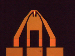
The new IBM tip offers lower wear rate than conventional silicon tips and is 100X stronger company claims
IBM spins ultrasharp nanomanufacturing tool 100,000X smaller than a pencil tip
The new IBM tip offers lower wear rate than conventional silicon tips and is 100X stronger company claims
 IBM says it has developed a silicon carbide tip for nanomanufacturing applications that it claims is a thousand times more wear-resistant than current tool bits and 100,000 times smaller than a pencil tip.
IBM scientists say the the new tip can be used to fabricate all manner of bio sensors, for example for managing glucose levels in diabetic patients or monitoring pollution levels in water.
Off the wall: All hail: Inside the museum of nonsense
Developed by IBM Research- Zurich, scientists at the University of Pennsylvania and the University of Wisconsin-Madison the nano-sized tip wears away at the rate of less than one atom per millimeter of sliding on a substrate of silicon dioxide. That fact is important IBM says because silicon-used in almost all integrated circuit devices-oxidizes in the atmosphere, forming a thin layer oxide. Poor wear performance of the tip materials used so far, especially when slid against silicon oxide, have previously limited their usefulness for experimental applications, IBM said.
The new tip offers a much lower wear rate of conventional silicon tips and its hardness is 100 times greater than that of the previously state-of-the-art silicon oxide-doped diamond-like carbon tips developed by the same team last year, IBM stated.
"Compared to our previous work in silicon, the new carbide tip can slide on a silicon dioxide surface about 10,000 times farther before the same wear volume is reached and 300 times farther than our previous diamond-like carbon tip. This is a significant achievement that will make nanomanufacturing both practical and affordable," said Prof. Robert Carpick of the University of Pennsylvania in a statement.
To create the new tip, the scientists said they developed a process whereby the surfaces of nanoscale silicon tips are exposed to carbon ions and then hardened so that a strong silicon carbide layer is formed, but the nanoscale sharpness of the original silicon tip is maintained. Although silicon carbide has long been known as an ideal candidate material for such tips, the unique carbon implantation and galvanizing process made it possible to harden the surface while maintaining the original shape and ensuring strong adhesion between the hardened surface of the tip and the underlying material-similar to how steel is tempered to make it harder.
Aucun commentaire:
Enregistrer un commentaire